


-

- Production of Nanoparticle & Fabrication of New Materials by Controlling Multifunctional Structure
- Production of Nanoparticle & Fabrication of New Materials by Controlling Multifunctional Structure Long-term stable stacked CsPbBr3 quantum dot films for highly efficient white light generation in LEDs In recent years, how to express colors more vividly and naturally has been raised as a major issue among researchers in the field of display. Producing colors is decided according to the light emitting spectrum of each light emitting diodes (LEDs) presenting red, green, blue. If the light emitting spectrum has narrow full width at half maximum (FWHM), the purity of light emitting material will be improved which can produce more vivid images close to the nature’s colors when applying to display. In recent years, semiconducting metal halide perovskite quantum dots (QD) have become attractive for use in many applications due to their outstanding electrical and optical properties. Particularly, metal halide perovskite materials are suitable for application in white LEDs (WLEDs) and displays due to their wide color tenability (from 400 to 800 nm) with control of the bandgap, narrow full width at half maximum (FWHM) of the emission band (around 20 nm), and high photoluminescence quantum yields (PLQYs), as well as their low temperature synthesis process and low cost compared with inorganic luminescence materials such as phosphor. The research team proposed an efficient and simple method to improve the stability of CsPbBr3 perovskite QDs and developed highly efficient white LED. They successfully prepared fully inorganic CsPbBr3 perovskite QD films as the green-emitting luminescence material for white light generation. High quality CsPbBr3 perovskite QD films with a FWHM of 21 nm as well as a high absolute PLQY of 37.2% were obtained. This demonstrates that the prepared film is a potential candidate with highly desirable characteristics for both lamp and display technology. The highly efficient CsPbBr3 perovskite QD film with Sr2Si5N8 : Eu2+ phosphor is applied to an InGaN blue LED chip, which demonstrates the luminous efficacy of 67.93 lm W−1 under a forward-bias current of 20 mA. Finally, the bright CsPbBr3 perovskite QD film can be a new material in a wide range of applications such as in optoelectronic devices. This article was published in 2016’s November edition of the world renowned scientific journal, Nanoscale. Mesoporous Ni–Fe oxide multi-composite hollow nanocages for efficient electrocatalytic water oxidation reactions In recent years, because of depleting fossil fuels and environmental concerns, eco-friendly renewable energy conversion technologies based on sustainable energy sources have attracted tremendous attention, such as water splitting, CO2 conversion and fuel cells. Among them, Hydrogen (H2) fuel produced via the water splitting process using electrocatalytic and photocatalytic methods has been a widely considered candidate to solve energy and environmental problems due to its carbon neutral, abundant, and sustainable energy sources. As a clean and sustainable technique, electrochemical water splitting could supply a large-scale hydrogen source. The anode reaction, namely the oxygen evolution reaction (OER) is one of the main steps in electrochemical water splitting. However, the OER limits the whole water splitting reaction due to (1) issue with substituting metal based oxide materials (2) short lifetime. In order to resolve these problems, extensive research activities have focused on multi-composite transition metal (Ni, Fe, Mn, Co, etc.) oxides and hydroxides, perovskites, and carbon-based materials as candidate catalysts for water splitting. Using a simple two-step hydrothermal method and calcination process, SKKU research team demonstrated the synthesis of mesoporous NiO/NiFe2O4 multi-composite hollow NCs via Ni3[Fe(CN)6]2 PBA nanocube precursors. Such mesoporous NiO/NiFe2O4 multi-composite hollow NCs after 1h of calcination in air at 500°C demonstrate enhanced OER activity with a remarkably low Tafel slope (58.5 mV dec-1), a low over potential of 303 mV at a current density of 10 mA cm2, and excellent cycling stability in alkaline electrolytes, superior to most reported hierarchical structures of binary transition metal oxides/hydroxides. Moreover, further such synthetic approaches can be carried out to explore the potential application of mesoporous and hollow binary transition metal oxides for advanced performance energy conversion and storage. This article was published in the world renowned research paper, Journal of Materials Chemistry A on Feb. 28th.
-
- 작성일 2017-04-25
- 조회수 6550
-
- Prof. Jeong Ho CHO and his team derived excellent performances in wearable electronic devices
- Stretchable and Multimodal All Graphene Electronic Skin (by Dong Hae HO) We demonstrated all graphene–based transparent and conformable multifunctional E–skin matrix. The CVD–Gr was used as electrodes in the matrix, while GO and rGO were adopted as sensing materials. A simple lamination process dexterously integrated the humidity, temperature, and pressure sensors as a whole. Each sensor was sensitive to its relevant external stimulus, but not affected by the other two stimuli. Moreover, all the sensors could work simultaneously and indicate different stimulations individually. The distributions of the temperature, humidity, and pressure under figure pressing were represented in 2D color mapping. This work suggested a facile fabrication process combined with graphene derivatives to transparent and conformable E–skin application, which overcome the conventional complex E–skin fabrication process. Additional sensors and wireless communication units could also be integrated through this simple lamination process, which would greatly help to realize interactive and remote health care in the future. Utilization of various graphene derivatives as main components in E–skin could also open up a way to accelerate the industrialization of graphene. Link: http://onlinelibrary.wiley.com/wol1/doi/10.1002/adma.201505739/full Low-Voltage Complementary Electronics from Ion-Gel-Gated Vertical Van der Waals Heterostructures (by Yong Suk CHOI) Isolation of ultrathin layered materials with disparate electronic properties has prompted their integration into van der Waals heterostructures with unique properties for electronics. By employing ion gel dielectrics, we demonstrate here low-voltage complementary circuits comprised of n-type and p-type van der Waals heterojunction vertical field-effect transistors (VFETs). The n-type and p-type VFETs were fabricated from MoS2 and WSe2 layers on graphene, respectively, with gating achieved by a top ion gel dielectric. Due to the high specific capacitance of the ion gel dielectric, the work function of the underlying graphene and consequently the energy barrier for charge injection into the MoS2 and WSe2 layers, are widely tuned at low operating voltages. The resulting VFETs possess high on-state current densities (> 3000 A cm-2) and on/off current ratios (> 104) in a narrow voltage window (< 3 V). In addition to enhancing VFET device metrics at reduced operating voltages, the high specific capacitance of the ion gel dielectric allows unprecedented regimes of charge transport to be accessed including p-channel phenomena in graphene-MoS2 vertical heterostructures. Furthermore, since the ion gel-gated VFETs possess low threshold voltages, a low-power complementary logic inverter is demonstrated using n-type and p-type VFETs. Overall, these results demonstrate the feasibility of vertical van der Waals heterostructures for high-performance, low-voltage electronics. Link: http://onlinelibrary.wiley.com/wol1/doi/10.1002/adma.201506450/full An Organic Vertical Field-Effect Transistor with Underside-Doped Graphene Electrodes (by Jong Su KIM) We fabricated vertical Schottky barrier (SB) transistors based on graphene–organic semiconductor (p-type pentacene or n-type N,N′-dioctyl-3,4,9,10-perylenedicarboximide (PTCDI-C8)) heterostructures. The Schottky barrier formed at the vertical graphene-organic semiconductor heterojunction could be modulated by tuning the applied gate voltage. Interestingly, molecular dopants (p-type bis-(trifluoromethane sulfonyl) amine (TFSA) or n-type poly (ethylene imine) were inserted underneath the graphene layer, which we refer to as the underside-doping method. This doping method enabled tuning the work function of the graphene while maintaining the surface properties of the graphene electrodes at the graphene-organic heterojunction, unlike when the dopants were placed on top of the graphene electrode (i.e. the topside-doping method). This charge injection at the heterojunction as well as the vertical transistor performances, including the device current density and on-off current ratio, varied systematically with doping the graphene electrode. The optimized p- and n-type devices yielded a high current density of 11 mA·cm–2 and a high on-off current ratio of ~103. Complementary inverters were successfully fabricated by assembling the p-type and n-type vertical SB transistors. The proposed underside-doping method opens up new opportunities for realizing future organic electronics. Link: http://onlinelibrary.wiley.com/wol1/doi/10.1002/adma.201505378/full Organic Dye Graphene Hybrid Structures with Spectral Color Selectivity (by Yu Sung GIM) This study characterizes a hybrid structure formed between graphene and organic dye molecules for use in photodetectors with spectral color selectivity. Rhodamine-based organic dye molecules with red, green, or blue light absorption profiles are deposited onto a graphene surface by dip-coating. UV–vis absorption spectroscopy, charge transport measurements, and density functional theory based calculations reveal that the photoresponses of the dye graphene hybrid films are governed by the light absorption of the dye molecules and also by the photo-excited-charge-transfer-induced photocurrent gain. The hybrid films respond only to photons with an energy exceeding the band gap of the immobilized dye. Dye-Graphene charge transfer is affected by the distance and direction of the dipole moment between the two layers. The resulting hybrid films exhibit spectral color selectivities with responsivities of ≈103 A W−1 and specific detectivities of ≈1010 Jones. This study demonstrates the successful operation of photodetectors with a full-color optical bandwidth using hybrid graphene structures coated with a mixture of dyes. The strategy of building a simple hybrid photodetector can further offer many opportunities to be also tuned for other optical functionalities using a variety of commercially available dye molecules. Link: http://onlinelibrary.wiley.com/doi/10.1002/adfm.201601200/full Mechanically Robust Silver Nanowires Network for Triboelectric Nanogenerators (by Hyung Seok KANG) The authors develop a mechanically robust silver nanowires (AgNWs) electrode platform for use in flexible and stretchable triboelectric nanogenerators (TENGs). The embedding of an AgNWs network into a photocurable or thermocurable polymeric matrix dramatically enhances the mechanical robustness of the flexible and stretchable TENG electrodes while maintaining a highly efficient triboelectric performance. The AgNWs/polymeric matrix electrode is fabricated in four steps: (i) the AgNWs networks are formed on a hydrophobic glass substrate; (ii) a laminating photocurable or thermocurable prepolymer film is applied to the developed AgNWs network; (iii) the polymeric matrix is crosslinked by UV exposure or thermal treatment; and (iv) the AgNWs-embedded polymeric matrix is delaminated from the glass substrate. The AgNWs-embedded polymeric matrix electrodes with four different sheet resistances, controlled by varying the AgNWs network deposition density, are deployed in TENG devices. The authors find that the potential difference between the two contact surfaces of the AgNWs network-embedded polymer matrix electrodes and the nylon (or perfluoroalkoxy alkane) governs the output triboelectric performances of the devices, rather than the sheet resistance. Both Kelvin probe force microscopy and numerical simulations strongly support these observations. Link: http://onlinelibrary.wiley.com/wol1/doi/10.1002/adfm.201603199/full Multibit MoS2 Photoelectronic Memory with Ultrahigh Sensitivity (by Da In LEE) Taking advantage of the superlative optoelectronic properties of single-layer MoS2, we developed novel MoS2 optoelectronic memory devices in which single-layer MoS2 films with a direct band gap of 1.8 eV were utilized as both the channel material and the light absorption layer. The advanced transfer method, benefitted from the adhesion-strained metallic layer, allowed us to obtain large-area high-quality single-layer MoS2 flakes that provided a phototransistor with ultrahigh sensitivity that exhibited a photoresponsivity of 8,024 AW–1 and a photodetectivity of 1012 Jones at an illumination power of 0.1 μW. In addition to the ultrahigh photosensitivity, the device memorized the number of incident photons in the form of a persistent current if gold nanoparticles (AuNPs) were used as the floating gates. Electron transfer from the AuNPs, along with the Pauli blocking mechanism, prevented the photoexcited electron–hole pairs from recombining; therefore, the persistent current was proportional to the intensity of light incident on the device. Multilevel data storage of the incident photons could be modulated precisely by tuning the applied gate voltage and the photo-illumination power. The MoS2 photonic memory exhibited excellent memory characteristics, including a large programing/erasing current ratio that exceeded 107, multilevel data storage of 3 bits (corresponding to 8 levels), performance stability over 200 cycles, and stable data retention over 104 s. 6. Link: http://onlinelibrary.wiley.com/doi/10.1002/adma.201603571/full Piezopotential-Programmed Multilevel Nonvolatile Memory As Triggered by Mechanical Stimuli (by Qijun SUN) We report the development of a piezopotential-programmed nonvolatile memory array using a combination of ion gel-gated field-effect transistors (FETs) and piezoelectric nanogenerators (NGs). Piezopotentials produced from the NGs under external strains were able to replace the gate voltage inputs associated with the programming/erasing operation of the memory, which reduced the power consumption compared with conventional memory devices. Multilevel data storage in the memory device could be achieved by varying the external bending strain applied to the piezoelectric NGs. The resulting devices exhibited good memory performance, including a large programming/erasing current ratio that exceeded 103, multilevel data storage of 2 bits (over 4 levels), performance stability over 100 cycles, and stable data retention over 3000 s. The piezopotential-programmed multilevel nonvolatile memory device described here is important for applications in data-storable electronic skin and advanced human-robot interface operations. Link: http://pubs.acs.org/doi/abs/10.1021/acsnano.6b05895
-
- 작성일 2017-04-25
- 조회수 6480
-
- The 7th SKKU – KANEKA International Symposium 2017 will be held on March 31st
- The 7th “KANEKA/SKKU Incubation Center International Symposium 2017” will be held on March 31st (Friday) from 9:30AM at SKKU Natural Sciences Campus. Since the establishment of KANEKA/SKKU Incubation Center in 2010 with the financial support of KANEKA Corporation, SKKU and KANEKA have been working together on joint research in the field of electronic material technology, and this symposium is also a part of the joint-research. The event will start with an opening speech by Prof. Seong Hyeon YUN of Samsung Medical Center, followed by lectures in regards to “Self-assembled Supramolecular Nanosystems for Smart Diagnosis and Therapy of Intractable Disease” from Kazunori KAKAOKA of the University of Tokyo, as well as the Director of Biomedical Institute for Convergence at SKKU. Also, a special lecture from Prof. Masateru ISHIGURO (Seoul National University) in regards to the subject “The Japanese Asteroid Missions” will be delivered while other valuable lectures are also prepared from Prof. Tsutomu MIYASAKE (Toin University), Prof. Nam Gyu PARK (SKKU), Prof. Tae Woo LEE (Seoul National University), Prof. Emeritus Katsuhiko TAKAGI (Nagoya University), and Dr. Toshikazu YAMADA (AIST). No registration or fees are required, so we look forward to many people participating. Date: March 31st (Friday) 2017, 9:30AM ~ 17:30PM Location: Medical Building 1F Lecture Hall, Natural Sciences Campus
-
- 작성일 2017-04-25
- 조회수 6291
-
- Development of Omnidirectionally Stretchable and Transparent Graphene Electrodes
- Stretchable and transparent electrodes have been developed for applications in flexible and wearable electronics. For customer-oriented practical applications, the electrical and optical properties of stretchable electrodes should be independent of the directions of the applied stress, and such electrodes are called omnidirectionally stretchable electrodes. Prof. Ho Seok PARK reported a simple and cost-effective approach for the fabrication of omnidirectionally stretchable and transparent graphene electrodes with mechanical durability and performance reliability. The use of a Fresnel lens-patterned electrode allows multilayered graphene sheets to achieve a concentric circular wavy structure, which is capable of sustaining tensile strains in all directions. The as-prepared electrodes exhibit high optical transparency, low sheet resistance, and reliable electrical performances under various deformation conditions. Furthermore, computer simulations have also been carried out to investigate the response of a Fresnel lens-patterned structure on the application of mechanical stresses. This study can be significant to a large variety of potential applications, ranging from stretchable devices to electronic components in various wearable integrated systems. The research was conducted with the support of CAP business and published in one of the most world renowned research papers ACS Nano. The title of the study was “Omnidirectionally Stretchable and Transparent Graphene Electrodes.”
-
- 작성일 2017-04-25
- 조회수 6494
-
- Graduate School of Water Resources will hold a ‘Campus Asia Launching International Symposium’
- After organizing a consortium with Nagasaki University and Shandong University, SKKU’s Graduate School of Water Resources (Dean: Kyung Soo JUN) has been selected for CAMPUS Asia’s new business units, which receive support from the Ministry of Education. To celebrate its launch and to wish a successful operation, a ‘Launching Symposium’ will be held between Feb 2nd ~ 3rd at the Samsung Library Auditorium. At the symposium, professors from Nagasaki University and Shandong University will participate; 16 researches will be introduced and strategic plans for CAMPUS Asia will also be discussed.
-
- 작성일 2017-04-25
- 조회수 6736
-
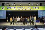
- 2017-1 Dean's List Award
- On April 5, 2017, The College of Engineering congratulated 225 honored students with outstanding academic accomplishments at Auditorium in the Samsung Library B1. On this day, the Dean of the College of Engineering introduced the “Dean’s List Award System” to honor students with passion and who have made great effort towards achieving scholastic excellence. Especially, students who got Dean's List award for 3 times got the special celebration with additional gifts. Dean LEE, Jun Young and the chairs of each School/Department conferred the Dean's List Awards with commemorative souvenirs. The purpose of the awards is to encourage students’ self-esteem as well as pride for their alma mater. There were department meetings, lab tours, and a graduate fair along with the award ceremony. Congratulatory letters were also sent to the parents of eligible students. Around 20 parents and relatives of the students awarded attended the ceremony which made it a much more meaningful celebration. The Dean's List Criteria are as follows: A. Semester - Students over 2nd semester of 3rd grade (6th Semester) [Architecture - 2nd semester of 4th Grade (8th semester)] B. Grade Point Average (GPA) - 4.0/4.5, including F grade C. Credits - Completed over 15 3 times Winner 4 Chemical Engineering 66 Advanced Materials Sciences & Engineering 38 Mechanical Engineering 75 Civil & Architectural Engineering and Landscape Architecture 11 Systems Management Engineering 20 Architecture 11
-
- 작성일 2017-04-10
- 조회수 6975
-

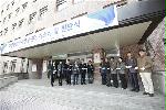
- Visiting from Addis Ababa Institute of Technology
- March 27th 2017, delegation from Ethiopia Addis Ababa Institute of Technology visited us and discussed about the future cooperation. Dr.Esayas (Vice President, Addis Ababa Universtiy), Dr.Daniel (Professor, Mechanical Engineering) and Byung-Soo, Lim met Lee, Jun-Young (Dean, College of Engineering), Roh, Yong-Han (Dean, College of Information and Communication Engineering) and chairs of the College of Engineering. And they discuss about cooperation between SKKU and AAiT in the area of technology.
-
- 작성일 2017-03-28
- 조회수 7127
-
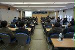
- 2017 1st Faculty Meeting
- "1st Faculty Meeting " was held in the 26106, Engineering Building 2 at 17:00, March 6th. In this meeting, the Dean, Jun-young, LEE awarded the appeciation plaque to the former Dean and Vice Dean. And, SKKU Fellowship professors and new professors was introduced.
-
- 작성일 2017-03-09
- 조회수 7411
-

- Graduation Ceremony in February, 2017
- The College of Engineering Graduation Ceremony was held on February 23rd, 2017 at the Auditorium in Natural Sciences Campus. Total 822 students received the certificate of graduation. The congratulatory speeches from Dean LEE, Jun-Young, president of an alumni association of the College of Engineering, LEE, Dong-Woo, parent representative Yoo, Byung-Chul and student representative KIM, Seok-Young were delivered. 9 students graduated summa cum laude with a degree in each school and department.
-
- 작성일 2017-03-09
- 조회수 7262
-
- The Opening & Signing Ceremony of ‘WE-UP: Women in Engineering – Undergraduate Leading Program’
- With the proposal of the subject ‘Smart Car’, SKKU was selected as one of the ten universities for ‘WE-UP: Women in Engineering – Undergraduate Leading Program’ project, which was organized by the Ministry of Education and the National Research Foundation of Korea. Many representatives including Ji Beom YOO (Vice-President of SKKU), Sung Jin SONG (Dean of College of Engineering), Byeung Woo JEON (Dean of College of Information and Communication Engineering), and Young Ik EOM (Dean of College of Software) attended the opening and signing ceremony on Dec. 12th to celebrate the opening of the ‘SMART WE-UP Center’. In the recent software-oriented industry structures, the need for women engineers has been rapidly increasing. However, due to the low number of women engineers, this need has not been fulfilled. Therefore, constitutional changes in the College of Engineering in regards to demonstrating women engineers’ talents and potential, as well as the cultivation of outstanding women engineers, are the most urgent issues. In regard of these needs, SKKU has chosen ‘Smart Car’ and established ‘SMART WE-UP Center’ which can create new converging business for women engineers. Sung Ho HWANG (School of Mechanical Engineering), the chair of the center spoke of his aspiration as “the future mobility industry will be led by the moving platform, Smart Car, which is the core area for value creation from the simple product. In order to lead the smart car convergence industry, engineers with soft sensitivity and social rising capabilities are in high demand and I hope the WE-UP center will play an important role.” At the congratulatory message, Ji Beom YOO, the Vice-President of SKKU said “Through this project, our university will take one step forward to becoming a ‘Truly, Global Leading University’, and I will provide active support if necessary.”
-
- 작성일 2016-12-28
- 조회수 7556